Industries
Semiconductors
Semiconductor Manufacturing Requires Precision. We Deliver It.
Built for cleanroom demands and tight-tolerance performance
Semiconductor equipment demands extreme precision, contamination control, and flawless process discipline — and MEP Technologies is structured to support exactly that.
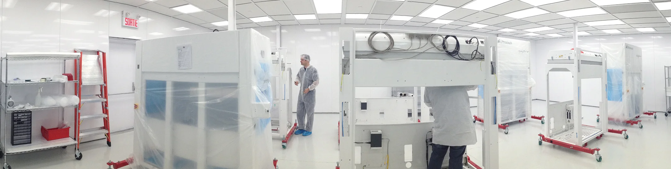
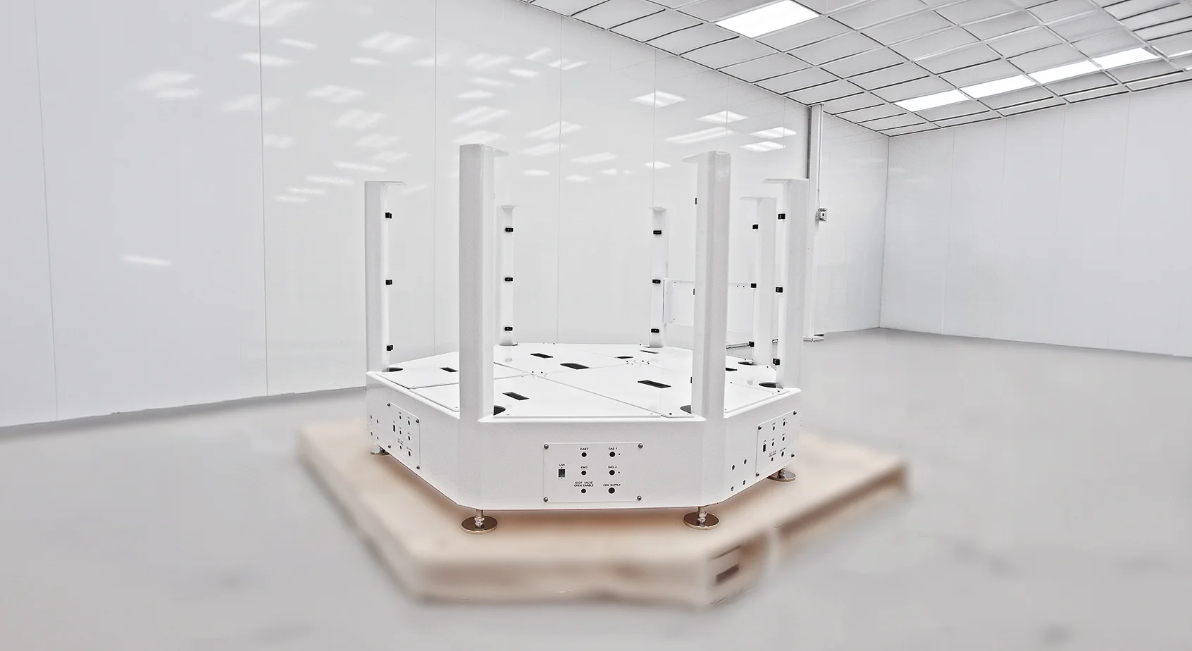
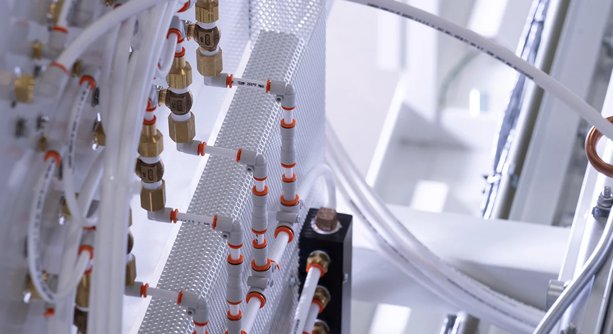
We integrate complex electromechanical assemblies built for particle-sensitive environments, tight tolerances, and multi-technology system requirements. With cleanroom capabilities, precision metal fabrication, and complete traceability under one coordinated organization, we help semiconductor innovators reduce risk, accelerate development, and bring high-value equipment to market with confidence.
Challenges in Semiconductor Manufacturing
The challenges semiconductor manufacturers face — and how we address them
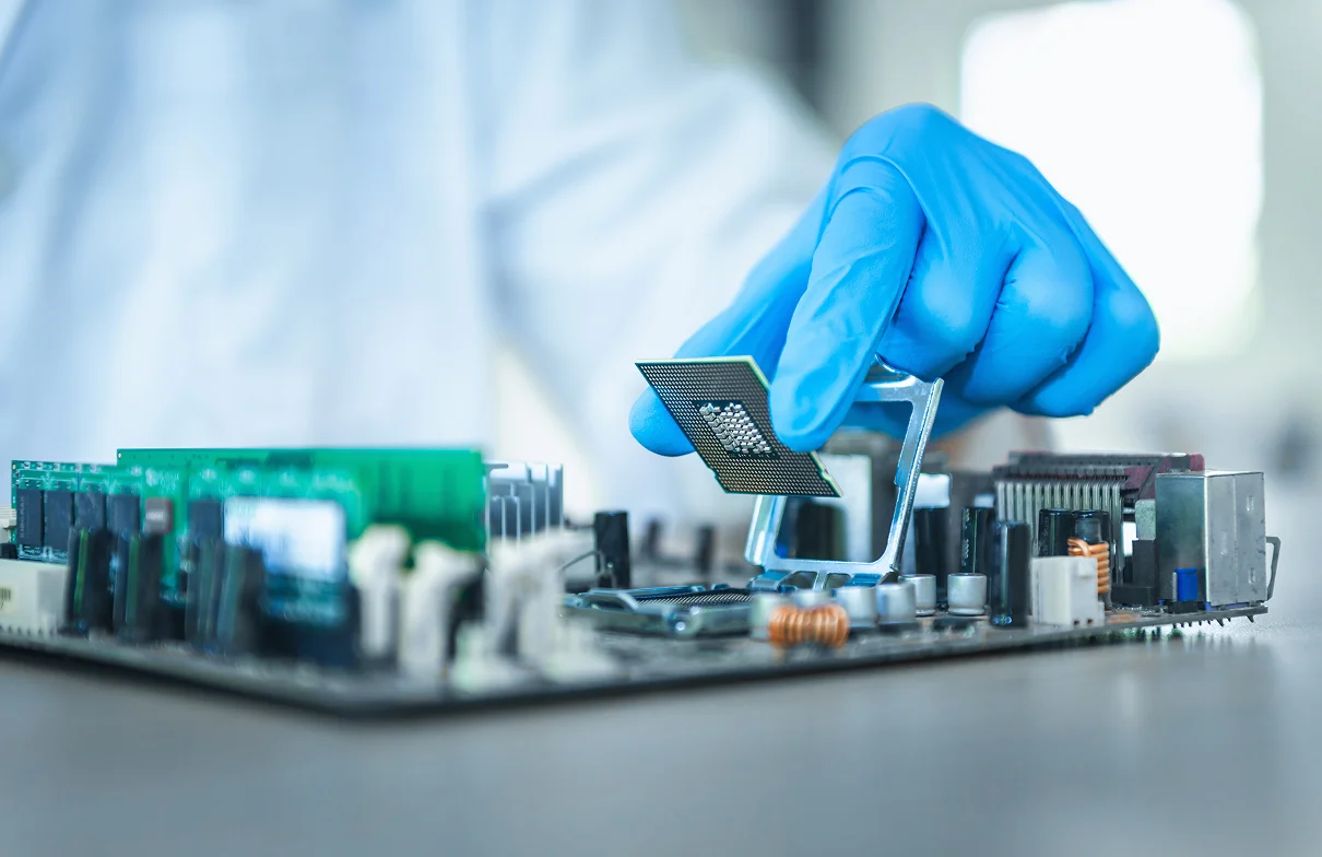
Semiconductor equipment builders operate under extreme demands: micron-level tolerances, particle-controlled environments, complex assemblies, and strict documentation requirements.
How MEP solves it:
Precision CNC fabrication, laser cutting, and controlled assembly processes designed for tight-tolerance structural and electromechanical components.
How MEP solves it:
ISO-classified cleanroom assembly, handled by trained teams following contamination-control procedures that safeguard particle-sensitive equipment.
How MEP solves it:
Mechanical, electrical, and electronic integration performed under one coordinated organization — reducing handoffs and eliminating multi-supplier risk.
How MEP solves it:
Full traceability systems, documented workflows, and complete FAI validation ensure compliance for regulated or high-reliability semiconductor equipment.
How MEP solves it:
Secure, controlled processes within four coordinated facilities, with no uncontrolled subcontracting and strong confidentiality protocols under Canadian jurisdiction.
Why MEP Is the Trusted Partner for Semiconductor Equipment
Developing semiconductor equipment requires more than precision — it requires a partner who understands the stakes: confidentiality, reliability, predictable throughput, and long-term support. MEP Technologies brings the structure, discipline, and partnership model needed to build complex semiconductor modules with confidence.
Why Choose MEP Technologies?
Contact usWe function as an extension of your engineering and operations teams, aligning with your workflows, documentation standards, and quality expectations.
We function as an extension of your engineering and operations teams, aligning with your workflows, documentation standards, and quality expectations.
We function as an extension of your engineering and operations teams, aligning with your workflows, documentation standards, and quality expectations.
We function as an extension of your engineering and operations teams, aligning with your workflows, documentation standards, and quality expectations.
We function as an extension of your engineering and operations teams, aligning with your workflows, documentation standards, and quality expectations.