Overview
A leading semiconductor equipment manufacturer required a new generation of large modular chamber structures for silicon wafer ion implantation systems. The project demanded a manufacturing approach capable of combining exceptional dimensional accuracy with innovative assembly concepts for rounded structural contours—requirements that exceeded conventional fabrication and assembly methods.
MEP Technologies developed new engineering and manufacturing approaches that enabled the successful production and assembly of these complex electromechanical structures while maintaining extremely tight tolerances across large modular assemblies.
The Challenge
Ion implantation equipment requires highly controlled environments where electrical safety, structural precision, and repeatability are critical.
The customer required chamber structures that presented several unprecedented manufacturing challenges:
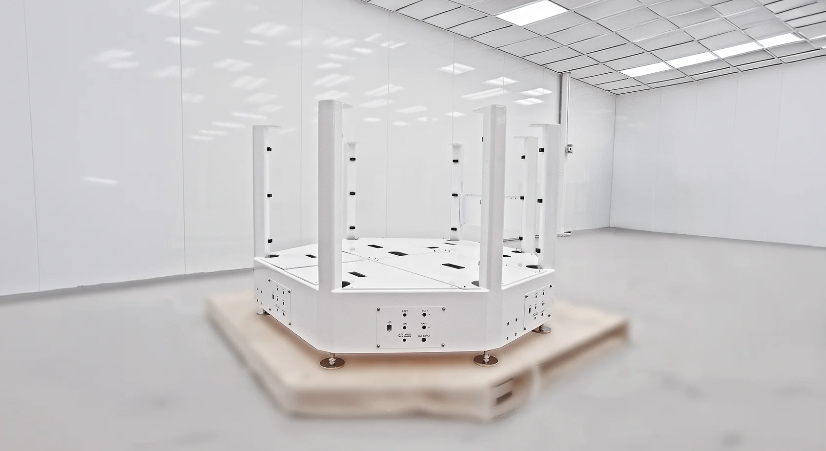
- Large modular assemblies measuring approximately 7.5 ft × 8 ft × 12.5 ft
- Overall dimensional tolerances of ±0.06 in, with critical features requiring ±0.03 in
- Rounded contours integrated along the entire external perimeter—not only at the corners—to minimize electrical arcing
- High-quality cosmetic finish with no visible deformation or fold marks
- Modular construction without compromising alignment during final assembly
Traditional fabrication techniques were not suitable. Standard methods rely on flat reference surfaces and separately formed rounded sections that are welded together—approaches that introduce distortion and prevent the required level of dimensional control.
MEP Technologies’ Approach
Rather than adapting existing methods, MEP Technologies developed entirely new fabrication and assembly concepts.
Advanced Forming Strategy
Our engineering team developed a manufacturing process capable of integrating conventional bends and rounded geometries within a single sheet-metal component.
Through extensive testing, we established optimal relationships between:
- Bending sequence
- Step-bending parameters
- Curvature radius
- Surface appearance
- Dimensional accuracy
This approach eliminated the thermal distortion associated with welding separately formed rounded sections while producing continuous rounded contours that met both structural and aesthetic requirements.
Precision Assembly Engineering
Conventional assembly fixtures rely on flat external reference surfaces—an option no longer available due to the rounded frame design.
MEP Technologies engineered a new fixture concept that:
- Used strategically positioned internal openings as reference datums
- Maintained structural rigidity while remaining lightweight and easy to handle
- Enabled highly repeatable positioning throughout the assembly process
- Controlled tolerance accumulation across multiple modules
The result was a modular assembly process capable of maintaining tolerances as tight as ±0.03 inches across the completed structure.
Optimized Assembly Sequence
The team also refined the complete assembly methodology by evaluating multiple module build strategies.
Key innovations included:
- Optimized temporary tack-weld placement
- Progressive module assembly from a stable base structure
- Mechanical joining strategies that minimized cumulative dimensional variation
- Controlled integration of individual modules into the final chamber assembly
Technical Innovations
The project generated valuable new manufacturing knowledge in several areas:
- Fabrication of complex sheet-metal geometries combining straight bends and continuous rounded contours
- Precision assembly methods for large modular structures without conventional flat reference surfaces
- Advanced fixture design for high-tolerance positioning
- Assembly sequencing techniques that minimize distortion and tolerance stack-up
- Manufacturing methods capable of achieving both cosmetic excellence and dimensional precision
Business Impact
By developing new manufacturing and assembly methodologies, MEP Technologies enabled the production of next-generation semiconductor processing equipment while maintaining the precision required for critical ion implantation applications.
The project demonstrates MEP Technologies’ ability to:
- Manufacture large, high-tolerance electromechanical assemblies
- Develop Design for Manufacturing (DFM) solutions when conventional methods are insufficient
- Support high-mix, low-volume semiconductor equipment manufacturing
- Deliver integrated manufacturing solutions for technically demanding OEMs
- Solve complex engineering challenges through collaborative manufacturing innovation